- 您现在的位置:买卖IC网 > Sheet目录2040 > PI74ALVCH162601A (Pericom)IC UNIV BUS TXRX 18BIT 56TSSOP
1
PS8093E 05/23/06
12345678901234567890123456789012123456789012345678901234567890121234567890123456789012345678901212345678901234567890123456789012123456789012
PI74ALVCH162601
18-Bit Universal Bus Transceiver
with 3-State Outputs
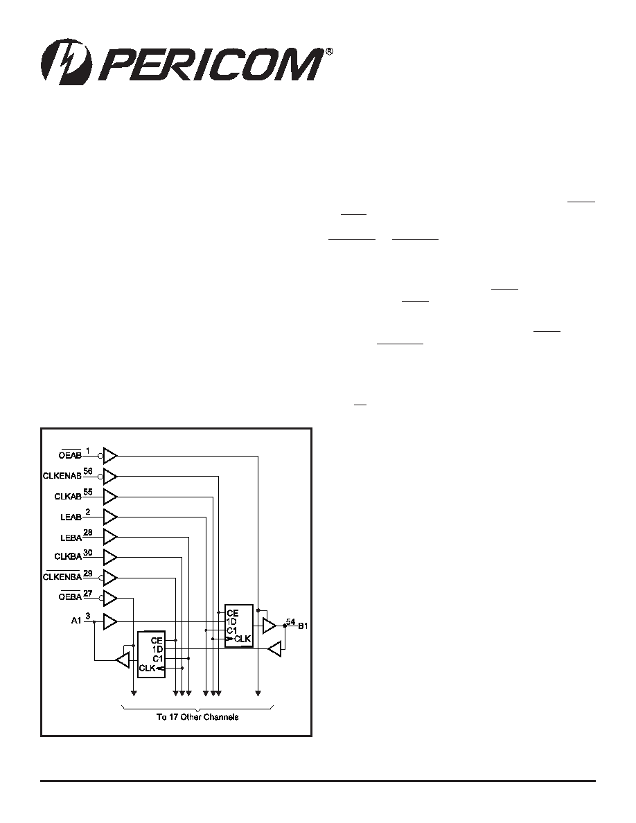
Logic Block Diagram
Product Features
Designed for low voltage operation, VCC = 2.3V to 3.6V
Hysteresis on all inputs
Typical VOLP (Output Ground Bounce)
< 0.8V at VCC = 3.3V, TA = 25°C
Typical VOHV (Output VOH Undershoot)
< 2.0V at VCC = 3.3V, TA = 25°C
Bus Hold retains last active bus state during 3-STATE,
eliminating the need for external pullup resistors
Industrial operation at –40°C to +85°C
Packages available:
– 56-pin 240 mil wide plastic TSSOP (A)
ProductDescription
The PI74ALVCH162601 uses D-type latches and D-type flip-flops
with 3-state outputs to allow data flow in transparent, latched, and
clocked modes.
Data flow in each direction is controlled by Output Enable (OEAB
andOEBA),LatchedEnable(LEABandLEBA),andClock(CLKAB
andCLKBA)inputs.TheclockcanbecontrolledbytheClockEnable
(CLKENABandCLKENBA)inputs. ForA-to-Bdataflow,thedevice
operates in the transparent mode when LEAB is HIGH. When LEAB
is LOW, the A data is latched if CLKAB is held at a high or low logic
level. If LEAB is low, the A-bus is stored in the latch/flip-flop on the
low-to-high transition of CLKAB. When OEAB is low, the outputs
are active. When OEAB is HIGH, the outputs are in the high-
impedance state.
DataflowforBtoAissimilartothatofAtoBbutusesOEBA,LEBA,
CLKBA,andCLKENBA.
To reduce overshoot and undershoot, the B-port outputs include
26
Ω series resistors.
To ensure the high-impedance state during power up or power
down, OE should be tied to VCC through a pull-up resistor; the
minimum value of the resistor is determined by the current-sinking
capability of the driver.
The PI74ALVCH162601 has “Bus Hold” which retains the data
input’s last state whenever the data input goes to high-impedance
preventing “floating” inputs and eliminating the need for pullup/
down resistors.
06-0134
发布紧急采购,3分钟左右您将得到回复。
相关PDF资料
PI74ALVCH16260A
IC 12/14-BIT MUX/LATCH 56-TSSOP
PI74ALVCH16501A
IC UNIV BUS TXRX 16BIT 56TSSOP
PI74ALVCH16646A
IC TRANSCVR DUAL N-INV 56TSSOP
PI74ALVCH16652A
IC 16-BIT BUS TXCVR/REG 56-TSSOP
PI74ALVCH16721A
IC 20-BIT FLIP-FLOP 56-TSSOP
PI74ALVCH16823A
IC 18-BIT INTERFACE-F/F 56-TSSOP
PI74ALVCHR162245AEX
IC TXRX 16BIT BIDIR 3ST 48TSSOP
PI74ALVTC16241A
IC BUFF DVR TRI-ST 16BIT 48TSSOP
相关代理商/技术参数
PI74ALVCH162601V
制造商:未知厂家 制造商全称:未知厂家 功能描述:18-Bit Bus Transceiver
PI74ALVCH16260A
功能描述:IC 12/14-BIT MUX/LATCH 56-TSSOP RoHS:否 类别:集成电路 (IC) >> 逻辑 - 锁销 系列:74ALVCH 产品变化通告:Product Discontinuation 09/Dec/2010 标准包装:1,500 系列:74VCX 逻辑类型:D 型透明锁存器 电路:8:8 输出类型:三态 电源电压:1.8 V ~ 3.6 V 独立电路:2 延迟时间 - 传输:1.5ns 输出电流高,低:6mA,6mA 工作温度:-40°C ~ 85°C 安装类型:表面贴装 封装/外壳:48-TFSOP(0.240",6.10mm 宽) 供应商设备封装:48-TSSOP 包装:带卷 (TR)
PI74ALVCH16260A56
制造商:未知厂家 制造商全称:未知厂家 功能描述:Bus Exchanger
PI74ALVCH16260V
制造商:未知厂家 制造商全称:未知厂家 功能描述:Bus Exchanger
PI74ALVCH16260V56
制造商:未知厂家 制造商全称:未知厂家 功能描述:Bus Exchanger
PI74ALVCH16269
制造商:未知厂家 制造商全称:未知厂家 功能描述:Logic | 12/24-Bit Registered Bus Transceiver
PI74ALVCH16269A
制造商:Pericom Semiconductor Corporation 功能描述:Registered Bus Exchanger 1-Element 56-Pin TSSOP Tube 制造商:Pericom Semiconductor Corporation 功能描述:ALVC/VCX/A SERIES, 12-BIT EXCHANGER, TRUE OUTPUT, 56 Pin Plastic SMT
PI74ALVCH16269V
制造商:未知厂家 制造商全称:未知厂家 功能描述:Bus Exchanger